Questions About Modifying & Troubleshooting
QUESTION. Can I use a different FET?
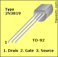
ANSWER. The 2N3819 works well in this circuit. Note the different pinout, though! (To make matters more confusing, some manufacturers reverse the source and drain leads. This page shows the Fairchild layout. Check your JFET manufacturer's datasheet!) Digi-Key and Mouser carry the 2N3819. Below are some other JFET types that might work in my circuit. (I make no guarantees, and haven't tried these parts.) Again, note that pinouts vary from FET to FET.
|
Using still other FETs might require circuit changes. “Replacement line” parts might or might not work. Also, such devices tend to be costly. To figure out your own substitution, check the device's datasheet. Can't understand it? Don't substitute. |
QUESTION. What's your technique for FET substitution?
ANSWER. Here's a start. Look for a match or near-match in these three datasheet parameters...
| • IDSS | • GFS | • Typical VDD |
Got your three-way match? You've probably found a sub! Buy a few of the matching parts and try them. Remember, no two FETs are exactly alike. For your tests, I suggest breadboarding the circuit on a component plug board. Radio Shack and other vendors sell the ideal model. Click... Plug board.
|
Get datasheets from... |
|||
| • Advanced Linear Devices | • Central Semiconductor | • Fairchild | • Infineon |
| • InterFET | • Linear Systems | • On Semiconductor | • SemiSouth |
| • Siliconix | • Solitron | • Supertex | |
QUESTION. Can you get me a schematic for a different preamp?
ANSWER. Sure. Use the Google "search" feature at the bottom of this page.
QUESTION. Can I run the preamp off some other voltage?
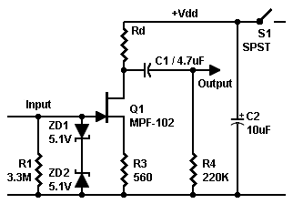
ANSWER. Yes. I've redesigned the bias circuit for the voltages below. These are the voltages that I recommend. Voltages below 9 volts are too low for most FETs. At 6 volts, you'd probably lose all your gain. Operation at more than 18 volts is probably too inconvenient for battery power. Anyway, you're getting close to the maximum for the FET, 25 volts. (Do you want to play through it, or detonate it?) For an MPF102, the ideal voltage is 15 volts.
Note that the source and gate resistors (RS and RG) remain the same as before. Just substitute the drain resistor (RD) below for the one in the nine-volt circuit...
|
|
QUESTION. The preamp doesn't work. Can you help me to debug it?
ANSWER. For $50 an hour, cash in advance, minimum $100, maybe. Anyway, save your money. Here are the usual problems...
- A reversed zener diode.
- Reversed FET pins.
- Static on the gate ate your JFET.
- The wrong resistor value.
- Wiring errors.
Also see our troubleshooting page.
QUESTION. I reversed the drain and source leads. Will this reversal cause a problem?
ANSWER. Don't worry. The MPF102 and 2N3819 are symmetrical JFETs. With each device, the drain and source leads are interchangeable.
Here's what's going on inside these parts: Each device has an channel that's a bar of N-material. The drain and source are terminals at the ends of this bar. In each device, the channel has a consistent width. The gate terminal connects at roughly the middle of the channel. You can think of the channel as a "hose." The gate functions as a variable "hose clamp," increasing or decreasing current flow through the channel.
I've built several 2N3819 amps with reversed drain and source terminals. (I had to do that to qualify for the "all thumbs engineer" award. Joking!) By the way, my "reversed" amps all work normally. Caution: If your circuit malfunctions, a drain-source reversal isn't the problem.
Beware! Not all JFETs and MOSFETs are symmetrical. For example, the substrate of some MOSFETs must connect to a dedicated source terminal. Also, some JFETs have gates that connect to the bottom of the channel. We call these JFETs "assymmetrical." Such devices operate best when you follow the manufacturer's drain and source connections.
|
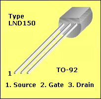
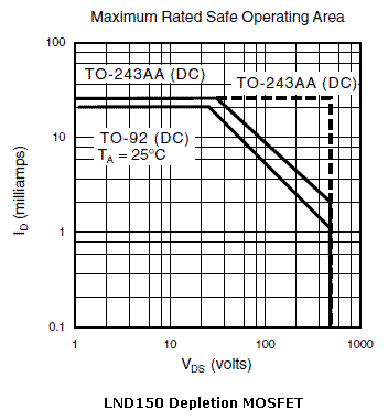
We could achieve a greater output swing by increasing the JFET's power voltage. We'd also have to adjust the drain resistor value and probably the source resistor value. Then we'll run into another problem: MPF102 JFETs can't withstand more than 25 volts. I don't recommend operating them above about 18 to 20 volts. I suggest a switch to a different device, the Supertex LND150 MOSFET. Buy the version in the TO-92, three-pin package (LND150N3-G). Buy several, because specs vary between devices. Also, when experimenting, you never know if you might lose a few devices. The LND150 can handle up to 500 volts. You can probably operate it with your tube power supply. Resistor and capacitor values are what you'd expect with typical guitar amplifier input tubes. A few precautions: The maximum voltage swing for an LND150 is plus of minus 20 volts. You must keep the gate swing below 20 Vpp. For this reason, I don't recommend using two LND150 stages. I suggest keeping the peak current as low as possible. I'll start my experiments with peak current at about 1 mA. See the nearby table. Use the bottom curve to determine the safe DC current level for the device. (I assume a TO-92 package.) For a 1 mA current level, here are the approximate part values... |
|
| Your B+ Voltage | Gate resistor | Drain resistor | Source resistor | Input & output coupling capacitors | Source capacitor |
| 40 | 4.7 M | 39 K | 120—1.2 K | 0.02 μF | 470 µF |
| 70 | 4.7 M | 68 K | 120—1.2 K | 0.02 μF | 470 µF |
| 100 | 4.7 M | 100 K | 120—1.2 K | 0.02 μF | 470 µF |
| 200 V | 4.7 M | 220 K | 120—1.2 K | 0.02 μF | 470 µF |
| All resistors are half-watt types. Carbon, carbon film or metal film resistors are fine. Coupling capacitors: Use Mylar or polyester, 600V parts. The source capacitor type is electrolytic. Source resistor: Experiment. Use the value that produces the best tone. (See tested values below.) | |||||
Simulation. In Bill's simulation, the LND150 matched the performance of a 12AX7. Bill's 6BQ5 output now clips nicely. At more conservative input voltages, the LND150 amplifier produces good sine waves. Here are the maximum specs for the LND150...
| Device | Package | Resistance Drain-Source, Rds (on) | Drain-Source Breakdown Voltage | Continuous Drain Current | Power Disspitation, PD | Maximum Operating Temperature | Maximum Swing, Vpp |
| LND150 N3-G | TO-92 | 1 KΩ at 0 V | 500 V | 0.03 A | 740 mW | + 150° | 20 Vpp |
Breadboard. I breadboarded the circuit on June 7, 2010. During tests with an old Conar® tube power supply, I ran several resistors through the solderless breadboard. I started with a 1 mA maximum current, and parts as in the above table. The 1 mA circuit didn't respond to changes in the source bias resistor. I increased the current to just over 2 mA. Then the LND150 started to behave in a proper, tube-like manner. Yippee! The parts values below produced the best results. P.S. Does anybody out there remember Conar? If so, flash your NRI class ring!
| • TESTED VALUES (6-7-2010) | |||||
| B+ Voltage | Drain Voltage | Gate resistor | Drain resistor | Source resistor | |
| 234 | 122 | 3.9 M | 100 K | 330 Ω | |
Wow. Does this sound good! For more about the final LND150 amp design, click: Solid tube preamp.
QUESTION. What's the easiest way to design my own preamplifier? A trimpot in the drain circuit?
ANSWER. We've all read about the trimpot-in-the-drain technique. This is an astonishingly poor design method. You can sometimes make a FET work that way. Yet you might not arrive at a useful circuit. The drain trimpot method ignores the JFET's minimum saturation current. If you fail to operate the JFET above minimum current, the device becomes unstable or won't operate. Any practical load will cause drain voltage to fall to zero. Conversely, should you exceed the maximum IDSS, you'll demolish the JFET. Below is a simple, rule-of-thumb design method. (In the worked examples, I use 9-volt power. The average current is 2 mA.)
- Start with IDSS. For an MPF102 or 2N3819, the minimum IDSS is 2 mA. For longest battery life, use the 2 mA as your average (not peak) current. If you want to use more current, keep well under 10 mA. (That allows peaks to approach 20 mA, the maximum.)
- With Ohm's Law, find the total resistance of the source-drain circuit. At 9 volts: (4.5 / 0.002) or 2,250 ohms (2.2KΩ).
- At 9 to some 15 volts, three-fourths of the 2,250Ω becomes the drain resistor: For our 9-volt circuit, use 1.5KΩ. The 1.5K value keeps current slightly above our minimum, 2 mA. (Word to the wise: Don't use the three-fourths ratio for all power voltages.)
- One fourth of the 2,250Ω becomes the source resistor: For our 9-volt circuit, use 560 ohms.
- Select your gate resistor. It can be just about anything. For high impedance, 1 to 4.7M is typical. Lower resistor values pick up less noise. Higher resistor values produce a more sensitive circuit. If loading the previous stage concerns you, use a high-value resistor. Then the load will be very light.
- As necessary, add coupling capacitors to the input and output. Remember that with a JFET, the gate should never go positive. A coupling capacitor can prevent an external DC circuit from biasing the gate positive. If you use a 1M or larger gate resistor, a capacitor value can be less than 1 uF. Use a Mylar or polyester film capacitor. For the output capacitor, the value depends on the next stage's input impedance. Again, 1 uF won't get you into trouble. If you need more low frequencies, increase the capacitor value. If your input has no capacitor, add a gate-stop resistor. 68K ohms is typical.
- If you need more gain, decouple the source resistor. That means: Wire a capacitor across the source resistor. The capacitor's reactance at the desired bottom frequency should be 10 percent of the source resistor value. That's Greek for: If you want to reproduce bass notes, make the capacitor value large (hundreds of μF). Otherwise, a few tens of μF should do.
The method above is a rule-of-thumb technique. Don't expect this method to work for all circuits. Tweaking part values might be necessary. If you're uncomfortable with experimenting, this method isn't for you. Try a cookbook Web site instead.
|
QUESTION. Would a variable capacitor across the source resistor allow me to change the gain? (Question from Tom Norton, 2010) ANSWER. Yes. Adding a source capacitor would increase the gain. That's the good news. Now the bad news: If you're working with audio signals, you need a variable capacitor in the microfarad range. As far as I know, such large variable capacitors are unobtainable. (Maybe you could use a C-multiplier circuit, but that's another topic.) I strongly recommend adding a fixed capacitor across the source resistor. Appropriate fixed capacitors are available from many vendors, including Radio Shack. With the source capacitor, the gain will vary across the bandwidth. The higher frequencies will have the highest gain. You can experiment with capacitor values and achieve an appropriate treble boost. A bass boost is also possible. A 150 µF source capacitor would boost the gain by 10 times. This gain would extend down to 20 Hz, where the gain would roll off by three decibels. You'd probably notice the difference, because the gain would rise from between two and three to about 20. (These are best-case gain figures. I assume that the amplifier is working into an infinite load.) |
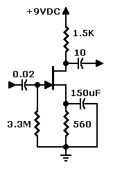 Bypass capacitor (treble boost), fixed. Click drawing for variable-gain circuit.
|
To vary the gain, you can bypass only part of the source resistor. Don't know how much gain you need? Replace the source resistor with a 500Ω potentiometer. Ground the bottom of the capacitor. Run the pot wiper to the top of the capacitor. Turning the pot will vary the stage gain. Word to the wise: The equalization will also change. That is, you'll get a variable treble boost and bass cut. To minimize the equalization effect, increase the capacitance.
If you want still more gain, increase the power voltage to 15 volts. Then use my 15-volt circuit on this FAQ page. The drain resistor will be larger, increasing your voltage gain. An 18-volt power supply would be fine, too. Please don't run the power up too much higher than that. The device turns into a pumpkin at 25 volts. (There's even a puff of smoke, but no bibbity bobbity boo.)
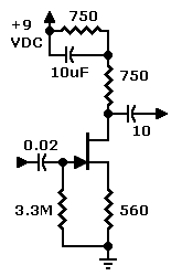 Bass booster, fixed. Click drawing for variable-boost circuit.
Don't know how much gain you need? Replace the drain resistor with a 1,500Ω potentiometer. Connect the top of the capacitor to VDD, the drain power supply. Run the pot wiper to the capacitor's negative terminal. Turning the pot changes the amount of bass boost from zero to maximum.
Go to Page: 1 2 3 4 5 6 7 Next
JFET Preamp Pages
- Introduction
- Schematic & Parts
- How It Works
- Spec Spread
- Improve Performance
- MPF102 in Tillman Circuit
- Troubleshooting
- FAQ