Spread in FET Specs
|
NOT UNIFORM. Unfortunately, FET behavior is anything but uniform. This statement is true even for FETs of the same brand and batch.
Characteristics that set the bias can differ by five to one! Meanwhile, the device still remains in spec.
Tubes and bipolar transistors are far more predictable. Manufacturers allow these FET specs to vary widely...
In fairness, specs of some FETs are tighter than for other FETs.
WHY DO WE CARE ABOUT SPEC SPREAD? If spec spread affects the device bias, then
the preamplifier might distort, or might not work. The source resistor sets the DC bias point (Vs). The input signal is a sine wave. This sine wave rises above and falls below the the bias point. Now let's consider the output at the device drain. Under no-signal (quiescent) conditions, we should find a DC voltage Vd between the drain and ground. This is the quiescent point (Q-point). The Q-point also depends on the DC bias setting. For example, when source bias rises, so does the drain Q-point.
Let's run a signal through the amplifier: The highest peak of the output wave can rise almost to the power voltage (Vdd). The lowest peak can fall almost to the device's source voltage peak. (In our case, excursions of Source Voltage Vs run a little above ground.) We want to set the bias point (Vd) about halfway between Vdd and average Vs. We make the setting under no-signal conditions. With a correct setting, we can amplify the signal a lot before the amplifier clips.
- Suppose that the bias point (Vd) is close to the top power rail. Then the amplifier might clip the top of the
waveform.
- Suppose that Vd is close to Source Voltage Vs. Then the amplifier might clip the bottom of the waveform.
- Suppose that Vd ("q-point") is halfway between the top power rail and Vs. Then we achieve ideal performance.
With spec spread, we can't say for sure where our bias point will be. We also don't know for sure if our design will clip
or not. Maybe the amplifier works, but we must avoid clipping by turning it down low. Obviously, spec spread affects the
predictability and quality of our project.
COPE BY TESTING. The preamp uses a typical MPF102 JFET. In this circuit, some MPF102s perform well. Yet others
might not operate at all. One way to cope with this problem is to hand-pick your JFETs. Here's how: Buy at least half a dozen FETs.
Check them in the circuit nearby.
For such tests, I recommend a plugboard. In twenty minutes, you can easily test several FETs and
weed out troublesome ones. Set aside devices that don't bias correctly. For example...
|
Set Device Aside
|
|
Vd Too High
|
Vd Too Low
|
|
Vd = 8.24
|
Vs = 1.74
|
Vd = 1.86
|
Vs = 1.53
|
|
Keep Device
|
|
Vd is 88% Perfect!
|
Vd is 99% Perfect!
|
|
Vd = 4.64
|
Vs = 1.59
|
Vd = 5.14
|
Vs = 1.40
|
|
|
Test of different JFETs
|
|
\
|
2N3819
|
MPF102
|
|
Test
|
Vd
|
Vs
|
Vd
|
Vs
|
|
01
|
4.24
|
1.74
|
4.86
|
1.53
|
|
02
|
4.84
|
1.52
|
5.38
|
1.33
|
|
03
|
4.06
|
1.81
|
5.12
|
1.43
|
|
04
|
4.20
|
1.75
|
4.83
|
1.54
|
|
05
|
4.27
|
1.73
|
4.49
|
1.66
|
|
06
|
5.38
|
1.32
|
5.53
|
1.28
|
|
07
|
4.75
|
1.55
|
5.26
|
1.38
|
|
08
|
4.55
|
1.63
|
4.74
|
1.57
|
|
09
|
4.61
|
1.61
|
4.85
|
1.53
|
|
10
|
4.64
|
1.59
|
5.14
|
1.40
|
|
11
|
5.00
|
1.46
|
4.33
|
1.72
|
KEY
- Vd = Drain voltage (between drain & ground)
- Vs = Source voltage (between source & ground)
|
Version of preamp to test spec spread
|
|
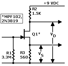
COPE BY TWEAKING. If you prefer, follow Tillman's advice and discard FETs that don't bias right. If you toss good parts,
though, you're throwing away money! Why not just make those leftover FETs work by tweaking the source resistor? Doing that adjusts
the bias. By adjusting bias, you can even improve performance of FETs that are close to the mark. See
How to Tweak the Source Resistor.
MY TESTS. I ran tests of comparable JFETs. For the tests, I used a plugboard. I wired up a
nine-volt circuit for the 2N3819. Then I copied the circuit for the MPF102. In succession, I plugged 11 devices into each circuit. Powering
on the circuit, I checked drain voltage drop (Vd) and source voltage (Vs) drop. Test results appear in the nearby table.
TEST RESULTS. Surprise! All of the tested devices would probably work in the JFET preamplifier circuit.
Yet all would not work equally well. The best devices have a Vd in the ideal Vd range, 5 to 5.5 volts. For this
circuit, the formula below computes the ideal Vd voltage. This formula provides an approximate result, not an
exact result...
|
|
Test Summary
|
|
Highest Vd
|
Lowest Vd
|
Difference
|
% Dif
|
|
5.53
|
4.06
|
1.47
|
36%
|
|
Examples of Ideal JFETs
|
|
\
|
2N3819
|
MPF102
|
|
Test
|
Vd
|
Vs
|
Vd
|
Vs
|
|
Ideal
|
5.30
|
1.60
|
5.25
|
1.50
|
|
4.5 + (0.5 * Vs) volts
DRAIN VOLTAGE TOLERANCE. Note that each JFET has its own ideal Vd voltage.
For the parts in the table above, the ideal ranges from 5 to 5.5 volts. If you're
within 10 percent of the ideal, then you're fine. Even 20 percent isn't bad. For example,
look at MPF102 #3. The ideal Vd for this part is 5.21 volts. I measured a Vd of 5.12
volts. This actual Vd is 98 percent of the ideal. I'd settle for that! If you don't like
the Vd, you can run a sound test. Or you can just tweak the source resistor. See...
Tweak.
BATCH SIMILARITIES. I purchased most of my test devices
in the same Mouser order. (The only exception is 2N3819 JFET #11.)
Maybe the devices in my order all came from the same batch. I'd expect same-batch JFETs to perform more alike than
different-batch JFETs. Anyway, don't assume that my results are typical. I have one 2N3819
with five times the gain of most of my other 2N3819 devices!
Go to Page:
1
2
3
4
5
6
7
FAQ
Next
|
JFET Preamp Pages
|