Experiment: MPF102 vs. J201 in Tillman Circuit
Objective
To find out if the MPF102 has any positive gain in the Tillman JFET preamplifier circuit.
Hypothesis
In the Tillman circuit, the MPF102 will attenuate (lose) signal strength, rather than amplifying.
Discussion
|
The Tillman JFET preamplifier uses a J201 JFET. Many builders substitute the more available MPF102 part. These builders usually leave the rest of the circuit as is. For more satisfactory operation, some people replace the source resistor with a potentiometer. This pot adjusts the JFET bias. By adjusting the pot, the user can set the amplifier's operating point for the lowest distortion output. Adding the pot is a means of coping with differences between the J201 and the MPF102. |
|
Bias isn't the only difference, though. Current is also very important. For best operation, the MPF102 requires at least four times the current that the J201 requires. For this reason, in the Tillman circuit, the MPF102 will probably attenuate. The Tillman circuit causes the MPF102 to operate outside its specifications. Operating the MPF102 this way will likely produce non-optimal performance. According to the datasheet, the MPF102 needs a minimum of 2 mA of current. The maximum current figure is 20 mA. The recommended voltage is 15 volts. The J201 is another matter. The J201 JFET works best at 10 volts. The minimum current is 0.5 mA. These are all ideal specifications. The specification spread of FETs is normally three to five times. I've personally seen a five-X variation in brand-name devices. The devices that I've recently tested are from the same batch. These devices perform more like one another.
I intend to operate the test circuits from a 9-volt, regulated power supply. My goal for proper bias of the MPF102 is 4.5 to 7 volts at the FET drain. If the MPF102 doesn't bias properly, I'll perform a second set of tests. In these tests, I'll take the MPF102 circuit and swap in source resistors. When I find a source resistor that produces drain voltage in the range, I'll rerun the source and drain voltage tests. Then I'll check to see if the MPF102 produces voltage gain or attenuates the voltage signal. If the drain resistor is substantially larger than the source resistor, the circuit has voltage gain. This statement assumes that when using these resistor values, the circuit biases the device correctly.
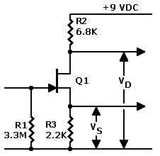
Procedure
I built the circuit on a plug board. Then I plugged in one test device. I powered the device and measured the drain and source voltages. I then replaced the test device with the next device of the same type, and repeated my tests. As I expected, I had to adjust the bias on the MPF102 transistors.
Results
The table below summarizes my results. I tested three of each type of JFET. For each transistor, the table has two columns. In the left column, I give the drain voltage. In the right column, I give the source voltage. Also note that I have a second "MPF102" column on the right. Under this heading are three columns. These three columns detail my adjustment to the MPF102 bias. The leftmost column is the new source bias resistor value. The middle column is the new drain voltage. The right column is the new source voltage.
MPF102 Performance in Tillman Circuit
| \ | J201 | MPF102 | MPF102 | |||||
| Device # | VD | VS | VD | VS | RS | VD | VS | |
| 1 | 7.68 | 0.41 | 2.90 | 1.95 | 8.2K | 7.07 | 2.43 | |
| 2 | 7.53 | 0.46 | 2.70 | 2.03 | 8.2K | 6.89 | 2.60 | |
| 3 | 7.46 | 0.48 | 2.69 | 2.03 | 8.2K | 6.85 | 2.61 | |
Table Key
- VD = Drain voltage, between drain and ground.
- VS = Source voltage, between source and ground.
- Rs = Source resistor value, in kilohms.
- Power voltage: 9 VDC, from regulated supply.
- Circuit: JFET with 3 carbon resistors (RG, RD and RS), on plug board.
- Devices: 3 of each type. Fairchild devices from same, 2007 Mouser Electronics order.
The output (drain) voltages on all three J201 FETs are above 7 volts. I'd expect all three to clip when the gate goes negative. Apparently all three devices have more gain than Tillman's J201 had. For better performance, a builder should decrease the source resistor. The source voltage will then drop, causing the drain voltage to drop, too.
In every test of the MPF102, the Tillman 2.2K source resistor was too small. This too-small value didn't produce enough voltage to properly bias the device. The output voltage of all three MPF102 devices dropped to around 2 volts. This voltage will guarantee clipping when the gate goes positive.
To correct the clipping problem, I provided a second set of MPF102 tests (right columns). In these tests, I increased the source resistor. I tried several resistors, with 6.8K producing about the best bias. (In one MPF102 test, VD = 6.6 volts and VS = 2.36 volts.)
| \ | MPF102 | ||
| Device # | RS | VD | VS |
| 1 | 6.8K | 6.60 | 2.36 |
To approach Tillman's results, though, I substituted an 8.2K source resistor. With this resistor, my drain voltages rose close to 7 volts. To match results from the J201, I'd have had to increase the source resistor even further. I could plainly see the trend. In any case, the high, 8.2K source resistor value causes signal attenuation. A larger value would attenuate even more. My preferred value of 6.8K produces an amplifier with a gain of just less than 1 (unity). This "best case" is a no-gain amplifier!
The voltage gain formula for these experiments is...
[ ( RD / ( RS + ( 1,000 / GFS ) ) * -1 ]
| RD & RS in ohms | GFS in millisiemens |
Conclusions
As the table shows, using an MPF102 in the Tillman circuit causes severe clipping. You can remedy the clipping by increasing the source resistor. Unfortunately, the new source resistor reduces gain to 1 or even attenuates the signal. The upshot: As an amplifier, the circuit fails. There are two ways to correct this problem...
- Decrease the source and drain resistors, allowing more current to flow through the JFET. Then adjust the source resistor for optimal bias and gain. For gain, the source resistor must be smaller than the drain resistor.
- Bypass the source resistor with a large-value, electrolytic capacitor. 100 to 1,000 μF should be sufficient. Unfortunately, the gain now varies across the bandwidth. An amplifier with a bypassed source resistor favors higher frequencies. In this circuit, all capacitors are high-pass filters. For better low-frequency response, use a large capacitor value. That's why I suggest a value as large as 1,000 μF.
Notes
Effect of Load. The voltage gain formula describes gain into a high-impedance (virtually infinite) load. In the real world, a load of less than some 100K affects the gain. As the load drops below 10 times the drain resistor, the gain decreases noticeably. Because the load parallels the drain resistor, the load must affect the gain.
Transconductance. Transconductance varies with the amount of current through the device. For the MPF102, the Fairchild datasheet gives the transconductance (GFS)as 2.0 to 6.5. But Fairchild measures these figures with 15-volt, 2 mA power to the device. In the Tillman circuit, the device average power is 9 volts at 0.5 mA. With such power, the MPF102 transconductance must be less than the datasheet spec. This lower transconductance further decreases preamplifier gain.
Go to Page: 1 2 3 4 5 6 7 FAQ Next
Index
- Objective
- Hypothesis
- Discussion
- Procedure
- Results
- MPF102 Performance in Tillman Circuit (table)
- MPF102 with 6.8K Source Resistor (table)
- Voltage Gain Formula
- Conclusions
- Notes
JFET Preamp Pages