JFET Preamp Pages
- Introduction
- Schematic & Parts
- How It Works
- Spec Spread
- Improve Performance
- MPF102 in Tillman Circuit
- Troubleshooting
- FAQ
Why an MPF102?
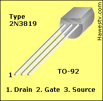
| It's available. Other Web designs use the Siliconix J201 or Motorola 2N5457. These are fine choices, but these parts aren't always available. The MPF102 is a common hobby part. It's reasonably easy to find, and should provide satisfying performance. You can buy one and get it working fast. (Unfortunately, Radio Shack doesn't carry the MPF102 anymore. But the compatible 2N3819 is still available from Mouser.com . You can buy either part at eBay. With eBay, look up a domestic parts source. Otherwise, expect l-o-o-o-n-g international shipping times!) |

|
|
|
|
It's durable. Also, the MPF102 is just as sensitive as these other devices, but probably a little more rugged. A J201 handles a maximum of 1 mA of current. The maximum for the MPF102 is 20 mA. Since FETs are very fragile devices, maybe the MPF102 has an edge. Maybe it will stay with you for a few years. Who knows how long you'll have a J201?
Low-Z output. With an MPF102, the output impedance is lower than with a J201. A little more power on the output means that your signal's a little stronger. You can probably drive a longer cable with the MPF102 than with the J201. (I haven't tested this idea.)
| / | MPF102 circuit | J201 circuit |
| Input impedance | Good: Very high | Good: Very high |
| Output Impedance | Good: 1500 ohms | Adequate: 6800 ohms |
| Voltage gain | 1.36 | 1.26 |
| Noise | Good: Very low | Good: Very low |
| Static resistance | Yes: zener | No |
| Battery life | Long | Very long |
| Parts cost | About $20 | About $20 |
| Easy to build | Yes | Yes |
| Online service instructions | Yes: Click Service | No |
| Adapts to other voltages | Yes. Click FAQ | No |
How It Works
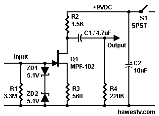
Power source. "Vdd" represents the power source for your JFET amplifier. The power source is a transistor radio battery. The battery provides nine volts to the drain of the JFET device, Q1. This voltage connects to the drain through drain resistor R2. The drain resistor is equivalent to the plate resistor in a vacuum tube circuit.
Common terminal. One terminal of this amplifier is common to both the input and output signals. This terminal is the JFET source terminal. For this reason, we sometimes call this amplifier circuit a “common-source circuit.” The circuit is equivalent to a grounded cathode tube circuit. Source resistor R3 connects the source to the battery's ground terminal. The source resistor acts like the cathode resistor in a vacuum tube circuit.
Class-A bias. The voltage drop across the source resistor also sets the JFET bias. Under no-signal conditions, bias voltage causes the JFET drain to draw a particular average current. This current sets the drain voltage at a point halfway between the Vdd voltage and ground. The name for this “halfway setting” is Class-A bias. This is the recommended bias setting for most small-signal, analog audio amplifiers. Class-A bias allows the maximum signal swing before distortion.
Voltage gain is low, an advantage because the preamp is unlikely to overload. The preamp's high-impedance input keeps the preamp from loading down the guitar and squashing your high frequencies. Here is the gain formula...
|
|
The signal enters the amplifier across gate resistor R1. Optional zener diodes Z1 and Z2 are a surge protector for the static-sensitive JFET gate. The zeners clamp when the input signal exceed 5.8 volts DC in either direction.
Signal and bias voltages. The voltage drop across R1 is the instantaneous input signal at the Q1 gate. This signal is an AC voltage. The signal enters JFET Q1, your amplifying device. The Q1 source is more positive than the Q1 gate. The difference is the voltage drop across resistor R3. Normally, the bias voltage across resistor R3 holds the JFET channel at a medium resistance value. The bias voltage is a DC voltage. When we apply a signal, the picture changes. Then the input signal varies the negative bias voltage across resistor R3.
How the JFET amplifies. The varying gate signal causes the JFET's channel resistance (or width) to vary. For this reason, more or less current passes through the JFET. Since the input signal controls the channel resistance, we've achieved valve-like operation. That is, a small signal controls a large signal. In our case, the Q1 gate voltage controls the Q1 drain current. This valve-like behavior is the basis of amplification.
External load. Resistor R4 is an optional, external load resistor. The purpose of this resistor is to keep the no-signal output of your amplifier from floating high. This unfortunate effect would only occur if the amplifier connected to a very high impedance without any resistance to ground. Although such connection is unlikely, it might occur. Of course, no advantages come without costs. For the signal, the R4 resistance shunts R2. That is, R4 is an extra burden for the JFET. For this reason, we keep R4 at least 10 times the size of resistor R2. A smaller R4 would seriously reduce the amplifier gain.
Transistor Sockets vs. Zeners
Go to Page: 1 2 3 4 5 6 7 FAQ Next
|
|||
|
Copyright © 2007 by James T. Hawes. All rights reserved.
•URL: http://www.hawestv.com/amplifiers/fet_preamp/fetpreamp3.htm
•Webmaster: James T. Hawes
|
|||