|
Step-by-Step Process
- Pick the gate resistor value (RG). Let RG equal the desired input impedance (Z). Don't know what resistance to use? Start with one megohm.
- Pick the power voltage (VDD) from the VDS values on the graph (right).
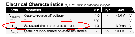
- Pick the maximum drain current ID. This value must fall between
zero milliamps and the device's IDSS value. (IDSS is the maximum
current through the device while shorting the gate and source. Manufacturers
specify IDSS as a range of values. For example, 1 to 3 milliamps.)
You'll find the range of IDSS values on the datasheet for your device.
Or: Look here: IDSS
Finder.
Don't know your device's exact IDSS value? Set ID to the
minimum IDSS value on the datasheet: For our example, 1 mA. This
value is likely one of the ID values for either IDSS
value. Also, 1 mA uses battery power economically.
- Draw the load line for your drain resistor. Run the line between the maximum power
voltage (VDS) and the maximum current (ID).
|
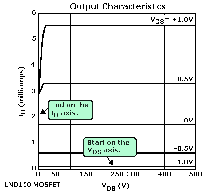
How to draw a load line. Mouse over the curves to see a load line.
|
|
- Find the drain resistor value (RD). Ohm's Law determines the drain resistor value: RD = (VDD / IS).
For example: (300 / 0.005) = 60KΩ → Use the closest, standard value. For example,
62K.
- Use the load line to select your bias curve. Halfway down the line is
the quiescent voltage. This is the drain voltage with no signal on the
gate. (Another name for this location is the Q-point.) On the X-axis, locate a point
midway between zero and the power voltage point. Draw a vertical from this point to
intercept your load line. With luck, this point will also intercept a bias curve.
(Your curve might not appear on the graph. Rest assured that your curve “is
there.” The engineer just didn’t draw it in. From two explicit, neighboring curves, you
may estimate your curve. You may then sketch in your curve.)
- Find the source resistor value (RS). The horizontal curve provides your bias
voltage value. Divide this voltage value by average current on the Y-axis. The result is your
source bias resistor value (approximately).
- Adjust the drain resistor value (RD). Does the source resistor value
exceed a tenth the value of the drain resistor value? No: Use a nearby standard
(RD) value within 20 percent. Yes: Subtract RS from RD.
The result is your new (RD) value. For both RD and RS,
use nearby standard values within 20 percent.
- Tweak the source resistor value. Usually the graph is too small to yield an exact resistor
value. Besides, actual device performance will vary from the graph. Some manufacturers provide maximum
and minimum graphs. Then you can come up with an average resistor value. Test this
value and tweak it for your best value.
How to Tweak Your Source Resistor
The Simulator Can't Find It for You!
♦Caution. Your Spice simulator can’t tell you the exact,
best source resistor value for your device. For years, this fact has been the crux of my frustration
with simulators.
|
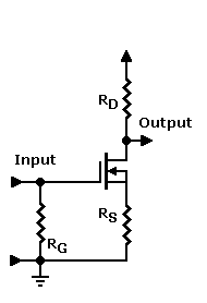
Amplifier schematic with standard resistor labels.
Mouse over image for standard voltage labels.
|
|
On a real circuit, you absolutely must tweak the source resistor value. If no
source resistor within 5X works, then the drain resistor value or B-plus voltage
is wrong. Or you have a lemon device. When I say “5X,” I mean a factor or
multiple of 5.
The best RS value produces a quiescent (no signal) drain voltage of approximately half the
power supply voltage. Yet: If (RS > 1/10 RD), the ideal VD exceeds
(1/2 VDD).
Load Line Design Example
|
The load line actually represents the sum of the drain and source resistors (RS + 1/10
RD). Let’s skip the source resistor for now. In this circuit, the effect of source resistor
RS is negligible. (RS only makes a difference when it’s
more than 10 percent the size of the drain resistor.)
- Pick the gate resistor value (RG). See above.
- Pick the power voltage (VDD). Suppose that you have a power voltage
of 234 volts.
- Pick the maximum drain current ID. For this example, the maximum current is 0.002
amp and change.
- Draw the load line between 234 volts on the bottom and 0.002A on the left. Now you have a
line whose slope stands for your resistor RD. The halfway point, 117 volts, is your Q-point.
(That's Q for “quiescent voltage point”: In the real world, it’s your “target” quiescent voltage.)
- Find the drain resistor value (RD). By Ohm’s Law, your drain resistor is close to
the standard value of 100K.
RD= (234 / 0.002) = 117KΩ → Use a nearby standard value within
20%. For example, 100K.
- Use the load line to select your bias curve. Your Q-point also intersects with your
bias voltage curve. For a depletion FET, the bias voltage at saturation is a horizontal line. If the line isn’t on the
graph, you may draw in the line.
- Find the source resistor value (RS). The intersecting bias
line (some -0.3 volts) is the source voltage drop. Remember that you drew the load line for maximum
current (ID). Dividing the bias line value by half this current gives you a ballpark source
resistor value.
ID / 2= 0.001
VS= 0.3V
(0.3 / 0.001) = 300Ω → Use a nearby standard value within 20%. For example,
330Ω.
- Adjust the drain resistor value. Our source resistor is much smaller than 10 percent of the drain
resistor. For this example, RD adjustments are unnecessary.
|
Draw the load line. To find the Q-point, roll over the drawing.
To find the source resistor value, roll over the drawing.
|
|
- Tweak the source resistor value. These small curve charts can't accurately pinpoint
the resistor value. Also, device variation will compel you to try neighboring resistor values. But the chart
will give you a starting point. (See above.)
Perfect Your Design
Got it working? Now get it perfect! Click... Tweak Your Amp Design.
|
Contents
Figures
|