Use Curves to Design Class-A Amplifiers
Almost No Math! With this method, you can design amplifiers with JFETs, depletion MOSFETs, and even triode tubes. In truth, you still need a little math. Yet if you slogged through a semester of high-school algebra, you'll do fine. If not, follow along. You might be in for a pleasant surprise. The process is simple: You draw over the manufacturer's drain (or plate) graphs. Then you apply Ohm's Law, which is a simple division, voltage divided by current. Two of the three resistor values for your circuit pop out. The third resistor is a given. Result: A Class-A amplifier schematic. Some electronic engineers use a more elaborate version of this same, graphic method.
♦CAUTION, Engineering Students. The design method on this page is just an introduction. This page isn't precise enough for your EE projects. If in doubt, ask your prof.
|
|
|
Study the DatasheetObtain the datasheet for your device from the manufacturer or catalog house Web site. For instance, Mouser and Digi-Key offer manufacturer datasheets. Examine the datasheet. Pay particular attention to the device's drain curve graph (“characteristic curves”). Here's how you'll recognize a drain curve graph: This graph has an X-axis (bottom) that represents drain voltage (VDS). The Y-axis (left) represents drain current (ID). Both axes present maximum and not quiescent figures. (See the example curve set at right.) If you can't obtain the datasheet, draw a rough graph similar to the figure nearby. Omit the horizontal lines, because they only apply to the LND150 device. Your drawing will help you to learn the process. Yet don't expect to design a working circuit: For example, your source-resistor value will be a complete guess. If you want to design circuits without using characteristic curves, click Design without curves! |
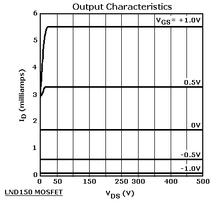
Drain curves for LND150 MOSFET. Mouse over for example of homemade graph. |
Contents
- Curve Design
- Prerequisites
- Study the Datasheet
- Introducing Load Lines
- What are curves?
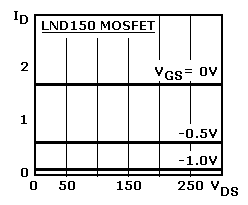
- Use the Negative Curves
- Step-By-Step Design Process
- How to Tweak Your Source Resistor
- Load Line Design Example
- Design an Amp Without Using the Curves
- FAQ
Figures
- Art: Supertex LND150
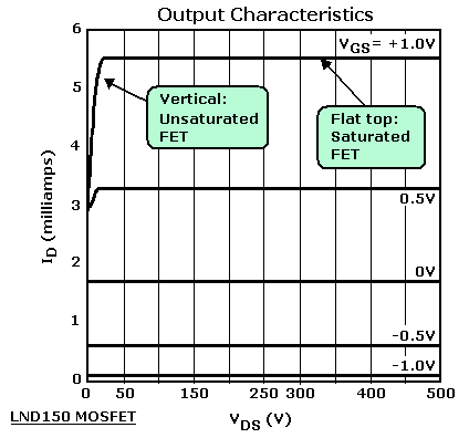
- Art: Curve family
- Art: Saturated region; negative curves
- Art: IDss value from datasheet
- Art: Load line
- Art: How to draw a load line
- Art: Amp schematic with resistor labels
- Art: Find the Q-point
- Art: Find the RS value