Hawes Amplifier Archive by James T. Hawes, AA9DT
Design a FET Amplifier Without Using Curves

Skip Intro

Gambling with Silicon Chips

Take the plunge. Designing without factory curves is a gamble. Know the risks: You might turn that junk box part into charcoal. On the other hand, you might well emerge with a working preamplifier. Consider this: If you don't try, all you have is a junk part. Whether the effort is worthwhile is up to you. I say “go for the gold!”

No-curve design is iterative. You try a resistor, take a measurement, and try a different resistor. To save time, you can build the circuit on a solderless breadboard (“plugboard”). Radio Shack and other vendors sell such boards. After a few experiments, you'll like the way the circuit performs. Then you can transfer it to perfboard or an etched PC board.

Prerequisites

  • Depletion Mode. The device must be a depletion-mode, silicon MOSFET or JFET. (No BJT transistors. No enhancement-mode MOSFETs. No GaAsFet, SiC or Ge devices.) For our examples, we'll use a Supertex LND150 MOSFET.

  • Source Bias. This technique works on source-biased ("self-biased") preamplifiers.

  • P-Channel FETs. This design process will work with N-channel or P-channel FETs. All examples refer to N-channel FETs, which are more common. To use a P-channel FET, reverse all power polarities. (For example, transpose the drain and source leads.) Also reverse all polar devices that connect to the FET. (For example, electrolytic capacitors and diodes.)

Diagram: Supertex LND150 in TO-92 package, showing pin layout
Supertex LND150

No-Curve Design Procedure

  1. Pick the gate resistor value (RG). Let RG equal the desired input impedance (Z). Don't know what resistance to use? Start with one megohm.

  2. Pick the VDD (power voltage) value. This voltage should run considerably below the maximum voltage for your device. If possible, keep the power voltage below half the maximum. Don't know the maximum? Go with a standard voltage: Many low-voltage FETs operate at 15 volts. Nine volts would then be fine. High-voltage FETs could top out at some voltage between 40 and 500 volts. Feeling lucky?

  3. Compute the quiescent drain voltage value (VD). Divide the power supply value (B+ or VDD) by two.

  4. Pick the quiescent (average) current (ID): Use as little current as necessary. Then the device will operate cool and use batteries economically. Usually a milliamp or two is a good starting point for tests. (For example: The minimum for the LND150 is 1 mA. For the MPF102, the minimum is 2 mA.) The device's IDSS values provide the best guidelines for choosing ID. Need help in finding your device's IDSS? Click: IDSS Finder.

Schematic with resistor labels. Mouse over for resistor values.

For parts values that I use, mouse over schematic.

  1. Compute the drain resistor value (RD). With tube-voltage circuits, the formula is...
    RD = (VD / ID).
    With low-voltage circuits (6 to 20 volts), the formula is...
    (RD + RS) = (VD / ID).

  2. Pick the source-resistor value (RS). If you're working with a high power voltage, try 1K. If you're working with a low power voltage, try one-third of RD. (Typical values run between 100 Ω and 5.6 KΩ.)

Art: Load line on graph of drain voltage & current. Mouse over to see load line.

You can graph drain voltage and current and then sketch in a load line. (Roll over.)

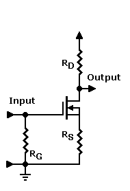
  1. Adjust the drain voltage. To adjust the voltage, tweak your source resistor value. The goal is to move drain voltage VD to half (or slightly more) of VDD.

    • Higher source resistor values (RS) “push” the drain voltage up.

    • Lower source resistor values “pull” the drain voltage down.


    You must adjust resistors in the real circuit. A resistor sub box is helpful here. (A couple clip leads and a Radio Shack resistor pack work even better.) Beware! Your PSpice simulator will never predict how the source resistor adjustment will go. After each resistor change, measure VDD. (Plugging in discrete resistor values is better than using a source pot. The pot value seldom corresponds to a standard resistor value.) Eventually you'll reach an RS value near the goal. You're done!

  2. Test your circuit under power.Touch the drain with an insulated alligator clip. Does the clip cause the drain voltage to collapse? If so, increase ID. Then recalculate and replace RD and RS.

Voltage Swing

It's All About Swing. Why are we so concerned about getting the drain voltage halfway to Vcc? Answer: To assure a maximum, undistorted voltage swing. That's why we want to move the quiescent (no-signal) drain voltage to about halfway between ground and B-plus.

Perfect Your Design

Got it working? Now get it perfect! Click... Tweak Your Amp Design.


Contents

Figures


Google Search
Web www.hawestv.com


WARNING. This is your project. Your achievement is entirely yours. I assume no responsibility for your success in using methods on these pages. If you fail, the same is true. I neither make nor imply any warranty. I don't guarantee the accuracy or effectiveness of these methods. Parts, skill and assembly methods vary. So will your results. Proceed at your own risk.

WARNING. Electronic projects can pose hazards. Soldering irons can burn you. Chassis paint and solder are poisons. Even with battery projects, wiring mistakes can start fires. If the schematic and description on this page baffle you, this project is too advanced. Try something else. Again, damages, injuries and errors are your responsibility. — The Webmaster


Copyright © 2010 by James T. Hawes. All rights reserved.

•URL: http://www.hawestv.com/amp_projects/design_page/fet_dsn_no_curves.htmWebmaster: James T. Hawes
•Revision—December, 2013  •Page design tools: HTML, Notepad & Explorer