IDSS Finder
Locate IDSS Characteristics for Various FETs
|
IDSS specifies the maximum current that can safely pass through the FET. Your amplifier design must fit into an “operation zone”: Maximum IDSS is the top boundary of this zone. The bottom boundary is minimum ID, which occurs at VGS (off). The left boundary is VP. The right boundary is the gate-source breakdown voltage V(BR)GSS. Stay well within these four boundaries, and you'll achieve a useful design. See the drain curves, right. The red rectangle represents the operation zone for a particular JFET. |
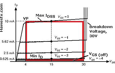
Fig. 1. Operation zone (in red) (1.) |
|
How to use the menus below. Start with your FET's part-number prefix or “family.” (For example, “2N-”.) Click the down button for this family. A menu drops down. Find your FET. For each FET, the approximate IDSS range appears to the right of the part number. All values appear in milliamperes. Where the manufacturer doesn't provide a value, you'll see “N/A” (not available). |
||
|
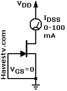
For IDSS ranges with unavailable values, estimate the IDSS value. For example, try “ballpark” values: For devices on this page, the average maximum IDSS value is six times the minimum. Example: The IDSS range is “2—NA.” The top number might be (2 x 6), or 12 mA. Measuring the IDSS is another possibility. You'll find a circuit for a basic IDSS meter at Figure 2. For more information on meters, see IDSS Tester & Tutorial.
|
|
|
|
▲ WARNING. The IDSS test is a momentary test. During IDSS current flow, some devices may become hot. Continuous operation at IDSS may damage such devices. (For example, a JFET in a TO-92 case with a 250 mA IDSS: It would probably require a heat sink for continuous operation.) Otherwise, your circuit might cause personal injury, and JFET damage is likely. |
How to use the values. To determine the quiescent drain current for your amplifier, pick a value within the IDSS range (min & max). Quiescent (no-signal) drain current must exceed the minimum ID value. Also, keep your value beneath the maximum.
IDSS Finder Table |
||
2N- Family |
2SK- Family |
BF- Family |
J- Family |
MPF- Family |
PN- Family |
Other Families |
P-Channel JFETs |
|
Footnotes
1. Albert Paul Malvino, Ph.D., Transistor Circuit Approximations, 3rd ed. (New York: McGraw-Hill Book Company, 1980), 236. ▶Re: Four drain-family curves. The “Operation Zone” drawing on this page derives from Malvino's drain curve drawing.
2. Idid., 235-236. ▶Re: IDSS refers to the drain current with the gate shorting to the source. This current is the maximum safe value of current. The IDSS measurement drawing on this page derives from Malvino's JFET bias drawing and his accompanying discussion.
Go to Page: 1 2 3 4 5 6 Next