Circuits that measure IDSS
|
It's not all there! What? Your parts manufacturer provides an incomplete IDSS range for your FET? Then he's telling you to go fish! What's a guy to do? You need some fishng gear. Homebrew an IDSS meter. Measure your FETs, instead of depending on incomplete datasheets. Sound good? Below are schematics for meters that reel in the data. |

|
|
♦ CAUTION. No enhancement devices. These circuits measure parameters for JFETS or depletion MOSFETs. But the circuits won't measure enhancement MOSFETs. If you plug in a MOSFET, it won't turn on. You might mistakenly assume that it's dead. (Examples: No 2N7000s! No BS170s!) |
About the meters
- Use your DVM for the ID ammeter and the VP (pinch-off voltage) voltmeter. The IDSS reading could vary from a few milliamps to about 100 mA. The power voltage that you use must exceed the FET's VP value.
- Your measurements apply to the device that you use, not the manufacturer's model. FETs of the same type vary greatly. (Sometimes nature intrudes upon science. FET characteristics are an example.) For this reason, your measurements probably won't agree with values on the manufacturer's datasheet. Fear not. Differing values don't indicate a defect.
- Battery considerations. IDSS-level drain current subjects your battery to the maximum current draw for the device. To preserve your battery, keep measurement periods brief. To measure P-channel devices, reverse the battery connections.
The simple meterBuild in minutes. Test in seconds! The simple IDSS meter (Figure 1) allows you to read IDSS. Depending on the FET you're measuring, IDSS could run anywhere from a few milliamps to 100 milliamps. (Very few FETs have an IDSS below 1 mA. Example: PN4117.) In this circuit, you may use a handheld multimeter to measure IDSS current. To find VGS (off), Malvino provides this handy formula (1.)... |
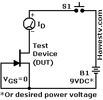
Fig. 1. Simple IDSS meter |
VGS (off)= 2(IDSS) / GM0,
where GM0 is the transconductance at IDSS
Why do I need to know VGS (off)? Because the pinch-off voltage VP is of the same magnitude (but opposite sign) as VGS (off). Manufacturers measure the all-important IDSS at the pinch-off voltage VP. Voltage VP also defines the voltage boundaries of your amplifier design (the most and least current that the FET supports).
Using the simple meter. The table below shows the results of some tests by the author. On a solderless breadboard, the simple meter circuit went together quickly. The 2N3819 device under test was a U.S. Fairchild JFET, originally from Mouser (new-old stock). The 2N5457 device was a Chinese “Fairchild” JFET from eBay. The readings were low, perhaps because the power voltage was 9 volts, instead of the manufacturer-specified 15 volts. To check that hypothesis, further tests were necessary. A retest several days later produced the same IDSS values at 9 VDC. Under 15 VDC power, the IDSS currents remained the same as at 9 VDC power.
The parallel IDSS values moderated the author's earlier skepticism about datasheets. The datasheet's drain curves prescribed that the IDSS values would be the same at 9 or 15 volts. The test devices regulated the current as they should. The measured IDSS values also remained within spec.
| FET Type | Power Volts | IDSS (mA) | Test Date | Tester Type |
| 2N3819 | 9 | 10.96 | 8-11-2020 | Simple |
| 2N5457 | 9 | 2.56 | 8-11-2020 | Simple |
| 2N3819 | 9 | 11 | 8-20-2020 | Simple |
| 2N5457 | 9 | 3 | 8-20-2020 | Simple |
| 2N3819 | 15 | 12 | 8-20-2020 | Simple |
| 2N5457 | 15 | 3 | 8-20-2020 | Simple |
• NOTES & CONCLUSIONS
|
||||
The swanky meterTechnician's Cadillac. The swanky IDSS meter appears at Figure 2. You can use the power voltage (B2) of your choice. The 20-volt supply is a typical example. (DC power packs are fine, too. A particular FET might also require a larger battery B1. For example, Hayes and Horowitz use -15V. (2.)) |
Fig. 2. Swanky IDSS meter (4.) |
To measure VGS (off), adjust the 10K pot. At some resistance value, the FET will cut off. When it does, ID will drop to zero. (Drain voltage VDS will also rise to the power voltage. (3.)) Now, measure VGS (off) between gate and ground. This circuit also allows you to plot the GM (transconductance) curve for the FET. (An example of this curve appears at Figure 5.)
|
♦ CAUTION: FIGURE 2. Never connect the gate battery B1 backwards! This battery must provide a zero to negative voltage to the gate. The voltage must never rise above zero volts. Otherwise, the gate junction could melt, destroying the JFET. |
Detailed instructions for the swanky meter
- Attach your DVM (M1) according to the schematic. (Connect the DVM "+" lead to VDD. Connect the DVM "-" lead to the drain terminal of the FET.)
|
Repeating Fig. 2. Swanky IDSS meter (4.) |
- After taking the reading, release button S1.
- To read VGS (off), connect a second DVM (M2) across the gate and common. (See the schematic, Figure 2.)
- Set your second DVM (M2) to read voltage.
- Reset pot VR1 to minimum current (opposite setting from what you used in Step 3).
- Press TEST BUTTON S1. At ID (M1), no current is flowing through the FET channel. The drain-to-ground voltage equals VDD (9 volts).
- While pressing the button, read VGS on M2. The reading will be in volts. The magnitude of this reading equals the pinch-off voltage VP. (Please ignore the sign. VP and VGS (off) use opposite signs.)
- After taking the reading, release button S1.
More About VP & IDSS
|
What is VP? VP, or more precisely, VP0, is the pinch-off voltage at IDSS. At VP0, the drain saturates with current. (5.) VP0 is equivalent to -1[VGS (off)]. (6.) See the drawing (right). What is IDSS? Looking at Figure 3, let's start at the origin, bottom-left. Moving right along the X-axis, we spot VP, the pinch-off voltage. Here, we arrive at the vertical line. Now, we follow the line upward to the drain curve IDSS. Here, we see that VP points to the knee in the curve. At this point, the current through the FET flattens out. We've reached current saturation, or IDSS! |
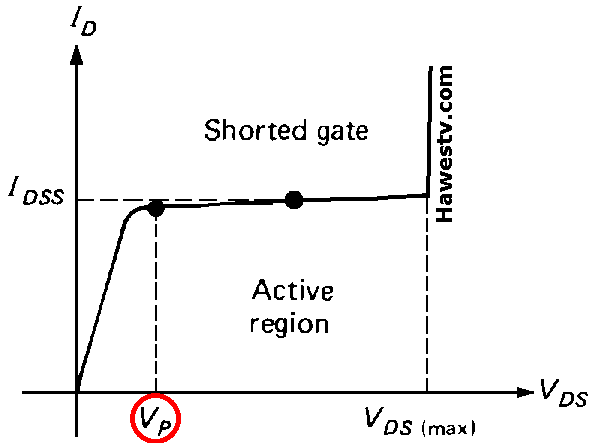
Fig. 3. IDSS occurs at pinch-off voltage VP. (7.) |
By “saturation,” we mean that the FET is passing the maximum current that it can safely handle. Going rightward from VP, the curve is flat. On the flat region, the FET operates as a constant current source. That is, drain voltage has almost no effect on drain current. (The device breakdown voltage is further to the right. At breakdown, the current rises exponentially. The device likely expires.) (8.)
Designing with Drain Curves
|
Flat section. On the device datasheet, there are more drain (ID) curves beneath the IDSS curve. Each drain curve has a saturation mode and a pinch-off voltage. We need the FET to operate on the flat, or “saturation mode” section of the curve. Select a drain curve. In design work, we can operate our FET on any drain curve. On Figure 4, right, the top drain curve is IDSS. Parallel to, and below IDSS are four horizontal curves. Each curve produces a different drain current ID. We identify these curves by the negative gate bias voltage VGS that produces them...
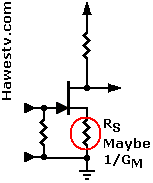
Deriving RS from GMSource resistor RS bias allows us to select a drain curve. RS bias reduces ID. A good, starting value for RS is (1 / GM). This statement assumes that we use the GM (transconductance) value at IDSS. (Datasheets sometimes refer to GM as GFS or YFS.) The datasheet provides GM as a range of values at IDSS. Yet we must choose only one GM value! We can cope by selecting an average or “typical” GM value. (Sometimes the manufacturer provides the typical value.) (10.) What is GM? There are two types of GM. Dynamic GM is the change in gate voltage that causes a given change in drain current. Static GM expresses the drain current per volt of gate voltage. The measurement is in amperes (or more likely milliamps). Yet we divide the ratio (mA / 1V) or (µA / 1V), expressing the result as a decimal number. The unit for this new term for inverse resistance is the Siemens, S (or U). Example: 3,000 µS or 3 mS. Both of these mean “3 milliamps per volt.” |
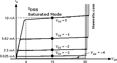
Fig. 4. Drain family curves
(9.)
Fig. 5. GM curve: RS selects drain curve.
(11.)
Fig. 6. RS & static GM |
|
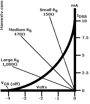
Source resistor connection. The reciprocal of any static GM value is a source resistor value. Malvino walks us through the easy RS formula. (12.) Be sure to ignore the VGS sign... RS= (-VGS / ID) RS examples. Figure 5 includes three examples of source resistors. The table below gives the calculations to find these three resistor values...
Tour of the GM Curve. At Figure 5, notice that transconductance (GM) is a parabola. As the curve ascends, the transconductance increases. As the curve descends, the transconductance decreases. Here's what this means for source resistor values: A large source resistor locks in a high reverse bias on the gate. With this gate voltage, the transconductance is low, but the current drain is economical. With this large resistor, be careful not to approach VGS (off) too closely, or the device might clip. A small source resistor allows far more drain current to flow. The transconductance is high, but the battery drain and heat might be excessive. A heat sink might be necessary. If the design approaches IDSS too closely, clipping could again become a problem. Consider the drain current of your circuit. Drain current affects the operating transconductance of the FET. Manufacturer specs usually give the transconductance figure at IDSS. Are you operating at a lower ID than IDSS? Then use a transconductance (GM) value that's less than the device maximum. Example: The manufacturer powers his model MPF102 at IDSS, 20 mA. But your project FET draws 2 mA, average. The datasheet GM range is 2 to 7.5 mS. You choose 2 mS, giving an RS of 500 ohms: (1 / 0.002)= 500Ω. You can then use a 470-ohm or 560-ohm standard resistor. |
VP & IDSS Summary
|
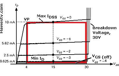
Fig. 7. Operation zone for a FET amplifier, within the active area of the drain curves. (14.) |
|
|
|||||||||||||||||||||
|
||||||||||||||||||||||
Go to Page: 1 2 3 4 5 6 Next
Footnotes
1. Albert Paul Malvino, Ph.D., Transistor Circuit Approximations, 3rd ed. (New York: McGraw-Hill Book Company, 1980), 239. ▶Re: Formula for finding VDS (off).
2. Thomas C. Hayes & Paul Horowitz, The Art of Electronics Student Manual, 1st ed. (New York: Cambridge University Press, 1989), 156. ▶Re: Use of -15V power supply to bias VGS. Useful when reading VGS (off). Broader range than 6-volt circuit in Kybett & Boysen. (Refers to measurement of N-channel devices. P-channel devices require a +15V bias supply.)
3. Harry Kybett & Earl Boysen, All New Electronics: Self-Teaching Guide, 3rd ed. (Indianapolis, IN: Wiley Publishing, Inc., 2008), 142. ▶Re: When there is no current flowing in the FET channel, VD rises to the power voltage VDD.
4. Ibid., 138. ▶Re: Schematic, circuit for measuring shorted gate drain current, IDSS & pinch-off voltage, VP.
5. Donald L. Schilling & Charles Belove, Electronic Circuits: Discrete and Integrated, 2nd ed. (New York: McGraw-Hill Book Company, 1979), 135. ▶Re: Term VP0, p. 136.
6. Malvino, 237. ▶Re: VP is VDS (off) without the sign.
7. Ibid., 235. ▶Re: Pinch-off curve diagram.
8. Ibid., 235-236. ▶Re: Connection between pinch-off voltage, VP, & shorted gate drain current, IDSS
9. Ibid., 236. ▶Re: Four drain-family curves.
10. Ibid., 239, 242-244. ▶Re: Good starting value for RS is (1 / GM), 242-244. •GM = GFS or YFS, 239. •Datasheets usually list GM at IDSS, 242 & 244.
11. Ibid., 236. ▶Re: GM or transconductance curves show how the RS value selects the drain curve.
12. Ibid., 236. ▶Re: Formula #2 for RS value: RS= (-VGS / ID).
13. Ibid., 236. ▶Re: When VGS = 0, you achieve IDSS, maximum drain current.
14. Ibid., 236. ▶Re: Operation zone for FET amplifier. The author drew the operation zone over a set of drain curves from Malvino.
15. Schilling & Belove, 135. ▶Re: The reverse-biased gate prevents gate current.
Contents
- Circuits That Measure IDSS
- About the Meters
- The Simple Meter
- The Swanky Meter
- Detailed Instructions for the Swanky Meter
- More About VP & IDSS
- Designing with Drain Curves
- Deriving RS from GM
- VP & IDSS Summary
- Footnotes
Figures
- Fig. 1. Simple IDSS Meter
- Fig. 2. Swanky IDSS Meter
- Fig. 3. IDSS
- Fig. 4. Drain Family Curves
- Fig. 5. GM Curve
- Fig. 6. RS & Static GM
- Fig. 7. Operation Zone