|
Skip Intro
Bring Out the Best in Your FET Amplifier!
Cut & Try. Congratulations! You've designed and built a depletion-FET (or tube)
amplifier, and it works. Now you need it to work even better. Maybe it doesn't have enough
gain, or maybe it clips due to excessive gain. Maybe the bias works, but the drain (plate)
voltage is too high or low. Maybe you want to change the frequency characteristics, reducing
or increasing low or high frequencies. This page helps you to cut and try modifications
until you get everything just right.
Prerequisites
- Depletion Mode. The device must be a depletion-mode, silicon MOSFET or JFET. (No BJT
transistors. No enhancement-mode MOSFETs. No GaAsFet, SiC or Ge devices.) For our
examples, we'll use a Supertex LND150 MOSFET.
- Source Bias. This technique works on source-biased ("self-biased")
preamplifiers.
|
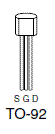
Supertex LND150
|
Definitions of FET Terms
|
Electrode
|
Capacitor
|
Resistor
|
Voltage
|
|
Gate (Grid)
|
Cg= Gate capacitor
|
Rg= Gate resistor
|
Vg= Gate voltage
|
|
Drain (Plate)
|
Cd= Drain capacitor
|
Rd= Drain resistor
|
Vd= Drain voltage
|
|
Source (Cathode)
|
Cs= Source capacitor
|
Rs= Source resistor
|
Vs= Source voltage
|
|
Power
|
Cf= Filter (anti-hum) capacitor
|
Rbl= Bleeder resistor
|
B+= Positive power voltage (tubes)
Gnd= Ground
Vdd= Drain power voltage
Vss= Source power voltage
|
Gain
Resistors Set Gain
Drain & Source Resistors. If you want voltage gain (Vgain), keep RS as small as practical in relation to RD.
RS must be large enough to “shove” VD up to at least half of VDD.
- If RS is 10 percent or less of the RD value, try for this: VD =
(VDD / 2).
- If RS exceeds 1/10 of RD, try for this: VD= [(1/2VDD) + (1/2 VS)].
- Need to reduce gain or improve fidelity? Increase your RS value.
If (RS = RD), you have a max gain of only 1. (In the real world, probably less.)
If (RS > RD), your circuit is degenerative. That is, lossy. Only with (RD
> RS) can you have gain. But only with VD = (1/2 or so * VDD)
can you have ideal linearity.
|
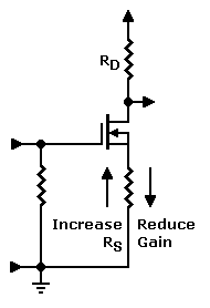
Reduce gain & boost fidelity: Increase the source resistor. (Roll over.)
|
Increase the Gain
|
Bypass the source resistor. By bypassing source resistor RS, you can use the perfect source resistor and still boost the gain. What do we mean by “bypassing”? We mean soldering a capacitor across RS. The capacitor will give a varying gain that increases as the frequency increases. On the low end, eventually the capacitor attenuates low frequencies. Larger capacitors allow lower frequencies to pass. The source capacitor formula is...
C = 1,000,000 / [2 Π * F * (RS / 10)]
Or this easier version: 160,000 / [(F * (RS / 10)]
where...
C is in microfarads.
F is in Hz.
Π is the constant pi ≈ 3.14.
RS is in Ω.
Example: For (F = 20 Hz) & (RS = 560 ohms): C = 142 μF.
Round up to a convenient standard value: 150 μF. 220 μF would also be fine.
Lower or higher cutoff. To extend the response to even lower frequencies, use a substantially larger capacitor size. To cut the low frequencies, use a substantially smaller capacitor size.
(For example: If 150 μF causes rolloff at 20 Hz, 1,500 μF will cause rolloff at 2 Hz. For a 200-Hz rolloff,
use 15 μF.)
|
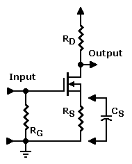
Boost gain: Bypass the source resistor. (Roll over.)
|
|
Fidelity
Getting too Much Distortion?
If you hear too much distortion and want a cleaner signal, consider reducing the gain. You can decrease the gain in
various ways. The easiest is just to remove the decoupling capacitor CS from source resistor RS.
Afterward, you'll notice much less distortion, because RS is degenerative. This resistor feeds back a small part
of the input signal, but out of phase. The out-of-phase signal counteracts distortion and makes the output signal more
linear.
If you lose too much gain when you remove the source capacitor, split the source resistor. Then bypass just
the bottom part of resistor. See the illustration at right. The unbypassed resistor will still cause degeneration. Yet
degeneration won't be as great as with a completely unbypassed source resistor.
Potentiometer method. Some builders substitute a pot for the source resistor. The wiper (center terminal) of the pot connects to the capacitor. Then these builders can dial in some intermediate level of gain. Unfortunately, this potentiometer method adds noise to the signal.
|
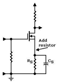
Roll over to see partial bypass of source resistor.
|
|
Coupling Capacitors for FETs
Please see our page on Coupling Capacitors.
|
Contents
Figures
|