Hawes Amplifier Archive by James T. Hawes, AA9DT
Convert Your Amplifier from Germanium to Silicon


Now, Let's Get Started...

Pick your germanium amplifier circuit from the types below. Then follow the instructions for converting your circuit. The changes affect the base-bias resistors. (See the drawing, right.) Round calculated resistor values to the nearest standard values. Since these are bias resistors, try to come within five percent. Single-ended amps are in the first group. Double-ended amps are in the second.

The examples below use NPN transistors. To convert PNP circuits, follow the examples, but reverse plus and minus power connections. Also reverse all polar parts (for example, diodes and electrolytics).

Schematic: bias resistors
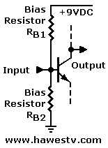
Schematic showing base-bias resistors

Words to the wise: Document your changes so that you can reverse them if necessary. Required skills: Desoldering, soldering and interpreting resistor values. Reading circuit voltages with a voltmeter. If you don't have these skills, please find a helper who does!

WARNING. The instructions below are general guidelines. Not every circuit conforms to these guidelines. Some circuits require special modifications that are beyond this page. Also, getting a circuit operating and getting it operating well aren't always the same. This page makes no claims about perfect operation after the conversion. You might still need to tweak the circuit. This page helps you to get the bias right. The gain, frequency response, noise level, sensitivity, etc. are your responsibility. Yet many times, a converted circuit will perform just fine. Notions of satisfactory operation are matters for your personal judgement. Example part values are only for reference. See other warnings and notices at the bottom of this page.


Single-Ended Amplifiers

  1. No bias resistors: Add resistor RB, base to Vcc. RB = (RC x (2 x beta))
    Notice: General-purpose, silicon transistors have a beta of about 200.

  2. 1 bias resistor RB: Replace with RB= same formula as A above.

  3. 1 bias resistor RB, returning to collector: Replace with RB = (RC x beta)

  4. 2 bias resistors, but no emitter resistor: Add new RB2= (former RB2 value x 2.3)
    Take care! The “2.3” multiplier is approximate. Some circuits require a slightly different value. Object: NPN base must be 0.7 volt positive. (PNP: 0.7 volt negative.)

  5. 2 bias resistors, with emitter resistor RE: RB= (((RE x IE) + 0.7) / (IE / 20))
    Where IE= ((VCC / 2) / (RC + RE): Ignoring internal RE= 26e-3 / Ie. The factor (IE / 20) above is both the current gain and stability factor (SF). SF can be as low as (IE / 1), that is, 1X. Typical SF is (IE / 10), or 10X. For reliable stability, avoid SF > 20X.

  6. 2 bias resistors and RE, with bypass capacitor: Same as E above.

  7. 2 bias resistors, RE, and Darlington circuit: Like E above, but use 1.4 instead of 0.7V. Also, Factor (IE / 20) can be 10% of beta. Conservatively, IE= 100 to 400. Sometimes more.

Schematic drawings depicting various
       germanium amplifier circuits and their equivalents in silicon; selectable by user


Double-Ended Amplifiers: Complementary Transistors

  1. Complementary transistors, with one silicon diode: Add a silicon diode in series with the other one.

  2. Complementary transistors, with two-diode bias: Replace germanium diodes with silicon types.

  3. Complementary transistors, with resistor bias: R3= (2 x ß x Load). (Assuming load= 8 Ω and ß= 70.) With no signal, the R4 value should be equivalent to two junction drops. For silicon, the total drop is some 1.4 volts. (Semiconductors vary, but typically no less than 1.2 volts.) Round to the nearest standard resistor value.

Schematic drawings depicting transistor
       complementary, germanium amplifier circuits and their equivalents in silicon; selectable by user


Double-Ended Amplifiers: Complementary Darlingtons

  1. Complementary Darlingtons with diode bias: Use four silicon diodes. The number of junctions between bases determines the number of diodes. With complementary Darlingtons, there are four junctions between bases. (The illustration shows how to count junctions. Note the “J1, J2, J3, J4” notations.) Instead of regular diodes, you may use a zener with the same voltage drop. One must reverse bias the zener. Regular diodes take forward bias.

  2. Darlington & Sziklai (inverting Darlington) with diode bias: Use three silicon diodes. The number of junctions between bases determines the number of diodes. From base to emitter, a Darlington has two junctions. From base to emitter, the pseudo-complementary Sziklai stage has only one junction. The total is three (not four) junctions between the two bases.

  3. Complementary Darlingtons with resistor bias: R3= (2 x ß x Load). (Assuming load= 8 Ω and ß= 1,000.) With no signal, the R4 value should be equivalent to four junction drops. For silicon, the total drop is some 2.8 volts. (Semiconductors vary, but typically no less than 2.4 volts.) Round to the nearest standard resistor value. Example "Si Version 2" is an adaptation of "Si Version 1." In Version 2, R3 & R4 pass the same current as in the germanium example.

  4. Darlington & Sziklai (inverting Darlington) with resistor bias: Germanium type: The voltage drop between bases is (0.3 volt x 3). Silicon type: The drop between bases is (0.7 volt x 3). Example "Si Version 2" is an adaptation of "Si Version 1." In Version 2, R3 & R4 pass the same current as in the germanium example.

Schematic drawings depicting Darlington
       complementary, germanium amplifier circuits and their equivalents in silicon; selectable by user


Double-Ended Amplifiers: Push-Pull

  1. Push-pull transistors or darlingtons with transistor phase splitter: Phase splitters may not require changes. If necessary: Provide sufficient forward voltage. This voltage must be 0.7 volt for silicon transistors, or 1.4 volts for Darlingtons.

  2. Push-pull transistors with transformer splitter: Be sure to provide sufficient forward voltage. This voltage must be 0.7 volt for silicon transistors, or 1.4 volts for Darlingtons.

Schematic drawings depicting various
       push-pull, germanium amplifier circuits and their equivalents in silicon; selectable by user


Go to Page:   1   2   3   4   5   6   7   Next

Article Chapters


Google Search
Web www.hawestv.com


WARNING. This is your project. Your achievement is entirely yours. I assume no responsibility for your success in using methods on these pages. If you fail, the same is true. I neither make nor imply any warranty. I don't guarantee the accuracy or effectiveness of these methods. Parts, skill and assembly methods vary. So will your results. Proceed at your own risk.

WARNING. Electronic projects can pose hazards. Soldering irons can burn you. Chassis paint and solder are poisons. Even with battery projects, wiring mistakes can start fires. If the schematic and description on this page baffle you, this project is too advanced. Try something else. Again, damages, injuries and errors are your responsibility.

WARNING. Power stages require adequate heat sinks. Power stages without heat sinks, or with inadequate heat sinks will overheat. As they become warm, transistors pass increasingly more current and may enter a thermal runaway condition. Thermal runaway can destroy transistors, start fires and cause property or personal damage.

CAUTION. A transistor amplifier with only one base resistor can be unstable. A transistor amplifier without an emitter resistor offers the advantage of low parts count. Yet due to thermal runaway, this amplifier might behave erratically. Even body heat from touching the transistor can significantly alter device gain. An emitter resistor can reduce thermal effects. This resistor also promotes better linearity and fidelity. The improvement is easily audible. — The Webmaster


Copyright © 2013 by James T. Hawes. All rights reserved.

•URL: http://www.hawestv.com/transistorize/germanium6.htm
Webmaster: James T. Hawes
•Revision—July, 2020
•Page design tools: HTML, Word, Notepad & Chrome