|
✪ CAUTION. This method only works with Class-A, R/C amplifier stages. Don't attempt to use this method on direct-coupled stages (except Darlington stages). If you do, you might upset the bias and end with a non-working or mis-biased circuit. This circuit will not perform as well as it did in the first place. |
Make That Amp Better
Amp doesn't work? Amp works poorly? You may have a bias problem. If so, this page can save you a lot of trouble.
Bias (bias voltage) allows an amplifier to reproduce both sides of a signal: The negative and the positive. Without bias, you only hear one side of the signal: Your amplifier clips. That's why one of the main objectives of amplifier design is achieving the ideal bias. Do that, and your amplifier will sparkle. You'll be proud. But without the right bias, the fidelity, gain, or stability will disappoint you.
Help is on the way! Proceed through the problem circuit one stage (transistor) at a time. Find the first preamp stage that you want to optimize. Match that stage to one of the schematics in our Bias Optimizer Tables 1 through 5, below. Breadboard the stage that doesn't work. Then follow instructions in the tables. When you get the breadboard to bias right, alter the original circuit to match your breadboard. Then optimize the next problem stage, if necessary. Follow the same process. Easy peezy!
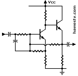
Measure the Vo: What's That?
|
Experiment. The Vo is the DC voltage output between the base of the top output resistor and ground. (The top output resistor goes by various names: Rc, Rd, or Rp.) You'll need to run some experiments and measure results with your voltmeter. Use the DC setting on your DVM, and measure the voltage with no signal on the amplifier input. The trick is that the Vo on your transistor, FET, or tube must be near half the power supply voltage. (1.) If not, the Bias Optimizer Tables tell you what resistors to swap out. (2.) (You may also use these tables with PNP transistors, and with P-channel FETs.) |
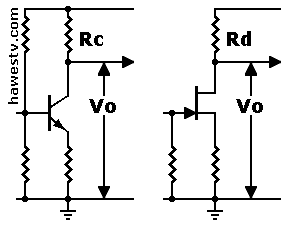
Measuring Vo (Left: In a BJT circuit. Right: In a JFET circuit.) |
|
♦ NOTICE. Not for voltage followers. This method will optimize working circuits that follow the schematics in tables 1 through 5. Only use this method on voltage amplifiers with gain. Don't use this method on voltage-follower circuits. This method affects the ratio of the top and bottom output resistor values. Followers don't have a top resistor. For that reason, this method is irrelevant to follower circuits. Use on follower circuits might downgrade circuit performance. |
Bias Optimizer Tables
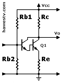
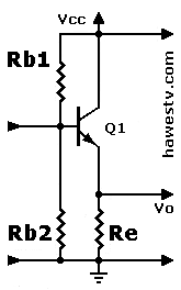
Table 1. BJT, Part 1 |
||
4-Resistor Circuit |
(Method also works with Darlingtons.) |
|
To Raise Vo*, Either. . .
—Decrease Swing —Cut V-Gain —Cut I-Gain |
To Decrease Vo*, Either. . .
—Increase Swing —Raise V-Gain —Raise I-Gain |
|
| *Increasing or decreasing bias resistor values might require other changes to the bias network. For example, increasing Re might necessitate a larger Rb2, a smaller Rb1, or both. | ||
Table 2. BJT, Part 2 |
|
2-Resistor Circuit(Inadvisable circuit) |
|
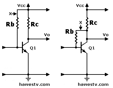
Never decrease Rc to less than 1/10 its original value.
If Q1 becomes hot, shut off circuit & increase Rc.
To Raise Vo, Either. . .
—Increase Swing —Raise V-Gain |
Before continuing, insert 1K current- limiting resistor at point “X” in circuit. To Decrease Vo, Either. . .
—Decrease Swing —Cut V-Gain |
Table 3. Depletion FETs |
|
3-Resistor Circuit |
|
To Raise Vo, Either. . .
—Decrease Swing —Cut V-Gain |
To Decrease Vo, Either. . .
—Increase Swing —Raise V-Gain |
Table 4. Triode Tubes |
|
3-Resistor Circuit |
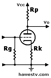
(Also works with tetrodes & pentodes.) |
To Raise Vo, Either. . .
—Decrease Swing —Cut V-Gain |
To Decrease Vo, Either. . .
—Increase Swing —Raise V-Gain |
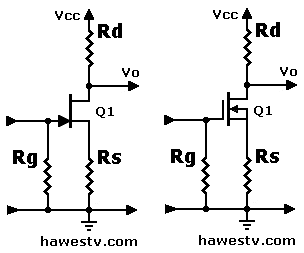
Table 5. Enhancement MOSFETs |
|
4-Resistor Circuit |
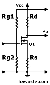
|
To Raise Vo*, Either. . .
—Decrease Swing —Cut V-Gain |
To Decrease Vo*, Either. . .
—Increase Swing —Raise V-Gain |
| *Increasing or decreasing bias resistor values might require other changes to the bias network. For example, increasing Rs might necessitate a larger Rg2, a smaller Rg1, or both. | |
Limits of This Method
|
✪ CAUTION. This method has limits. It can optimize most preamplifier circuits, but not all of them.
|
Terms for this section. . .
- References to the “collector” also refer to the drain or plate.
- References to the “emitter” also refer to the source or cathode.
- References to the “base” also refer to the gate or grid.
Discussion. The caution above refers to “limits.” Here are some examples of these limits. . .
- Problem of no gain.
Suppose that you can only achieve 50% bias on the collector by increasing the
emitter resistor until it equals the collector resistor. Then your circuit will only
provide a voltage gain of one. In this case, the method is incapable of optimizing
the circuit.
The remedy might be using a different amplifying device. Or perhaps substituting a different circuit that allows the device to pass more current. To achieve success with this new circuit, you might have to change all the resistors.
But there's hope. Must the gain descend all the way to zero Hz (DC)? If not, you can restore gain above a low frequency of say, 20 Hz. Do this by adding an emitter-bypass capacitor (Ce, right). (3.) Solder this capacitor across the emitter resistor (source or cathode resistor for some circuits). With the capacitor, the emitter resistor may be larger than the collector resistor. You'll still achieve voltage gain. But this gain will increase with frequency. The table below recommends capacitor values. Use a capacitor of appropriate voltage capability for your circuit. 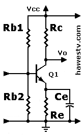
Use of emitter capacitor Ce
Suggested Values for Capacitor Ce Emitter Resistor Re 100-500Ω 500-1KΩ 1K-5KΩ 5K-10KΩ 10K-50KΩ Emitter Capacitor Ce (Bottom= 20 Hz) 820µF 180µF 82µF 18µF 8.2µF - Problem of too much gain.
Suppose that you can only achieve 50% bias on the collector by decreasing the
emitter resistor value to zero ohms. Then your circuit will produce its maximum voltage
gain (usually about 200 to 250), at its lowest input impedance. The circuit might also
become so unstable that it's unusable. In this case, the method is incapable of
optimizing the circuit.
The remedy might be using a different amplifying device. Or perhaps substituting a different circuit that allows the device to pass less current. To achieve success with this new circuit, you might have to change all the resistors. - Insufficient gain from the two-resistor circuit (Table 2): Suppose that you achieved 50% collector
bias. But correct bias didn't occur until the base resistor nearly equalled the
collector resistor value. Then your circuit might only provide a voltage gain of
one. In this case, the method is incapable of optimizing the circuit.
The remedy might be using a different amplifying device. Or perhaps substituting a different circuit. - Too much gain from the two-resistor circuit (Table 2): Suppose that you achieve 50% bias on
the collector. But now the circuit whistles (feeds back, oscillates).
In this case, the method is incapable of optimizing the circuit.
The remedy is a return to the original circuit. (Discretion is the better part of valor. Thank you, Falstaff.) - Other problems. Suppose that you changed a resistor, but voltage Vo remains the same.
You might have a wiring error, or a bad device. Please check to see that you inserted the
transistor, FET, or tube the right way.
A datasheet for your device is available online. Search for the device name (example: “2N2222”) and “datasheet.” You can also look up your part number at a vendor such as Mouser Electronics. Then click the “datasheet” icon for your part. Check the device pinout and make sure that you've installed the device correctly. Also check for wiring errors and open connections.
If the Vo is zero under power, you might have a leaky device. If you think a device is bad, replace it with a new device. Keep the old device in case you're wrong. Hint: A wiring error can mimic a shorted junction. A disconnected emitter, collector, or base can mimic an open junction. - A normal junction acts as a semiconductor.
- A shorted junction acts as a conductor.
- An open junction acts as a disconnected wire.
- A leaky junction acts as a resistor. Voltage appears across it.
|
✪ CAUTION. The two-resistor circuit (Table 2)
is fine for hobby purposes, or a few industrial applications. But this circuit
offers the lowest stability (by far) of any preamplifier circuit. (4., 5.,
6., 7.) Also, the two-resistor circuit produces
the highest distortion (8.) and
has the lowest impedance of any circuit on this page. |
Transistor Failure Modes
| Symptom | Location | Problem |
| Vo= Vcc | BE | |
| Vo= Ve | BC | Short / Leaky |
| Vo= Ve | CE | |
| Vo= Vcc | BE | |
| Vo= Vcc | BC | Open |
| Vo= Vcc | CE | |
|
KEY: B= Base. E= Emitter. C= Collector. BC & BE are the two junctions
inside the device. CE is the operative current path across both junctions.
|
||
|
♦ NOTICE: Distortion Circuits. If you wish to build a distortion or “overdrive” circuit, follow tables 1 through 5 in reverse. For example, when the table specifies “Increase Re”, reduce Re instead. |
Glossary
Amplifier Terms
- Bias. (Also bias voltage.) Bias allows an amplifier to reproduce both sides of a signal: The negative and the positive excursions. Without bias, you only hear one side of the signal. That is, your amplifier clips. With few exceptions, discussions of “bias” on this page usually refer to forward bias.
- Bypass capacitor (Also Ce, CE.) An capacitor that increases stage gain by detouring the AC signal around the emitter resistor Re. (The emitter resistor is degenerative.) There are costs for using this capacitor...
- Circuit complexity and reliability.
- Circuit stability.
- Reduced input impedance at lower frequencies.
- Gain with capacitor varies with frequency.
- Narrows bandwidth of amplifier.
- Causes a high-frequency cut.
- Ce. (Also bypass capacitor, CE.) An optional bypass capacitor across emitter resistor Re. (Don't confuse Ce with “CE”!)
- Class A. An analog amplifier where amplifying device remains on constantly. Amplifier output precisely follows input. The highest in fidelity and lowest in efficiency of amplifier classes. A typical circuit for high-impedance, high-fidelity preamplifiers.
- Forward bias. A bias voltage that turns the transistor halfway on. That is, the bias turns on the BE junction, but not the BC junction.
- Reverse bias. A bias voltage that turns off the transistor. That is, the bias turns off the BE junction.
- R/C. (Also R-C or RC.) Resistance coupled, or resistance-capacitance. Refers to method of connecting one amplifier stage to another. R/C amplifiers couple through resistors to power rail, with capacitor between these resistors.
| Other Names for Bypass Capacitor | ||
| In BJT Circuit | In JFET/DMOS/EMOS Circuit | In tube Circuit |
| Ce | Cs | Ck |
Transistor Terms
- Base, b. One of three electrodes on bipolar transistor. Usually input.
- BC. Base-collector junction of a bipolar transistor (BJT). This junction is a diode. In circuits on this page, we seek to reverse bias the BC junction.
- BE. Base-emitter junction of a bipolar transistor (BJT). This junction is a diode. In circuits on this page, we seek to forward bias the BE junction.
- BJT. Bipolar junction transistor transistor. Called “bipolar” because it conducts in two directions: Within the device, holes and electrons flow in opposite directions.
- CE. The connection across both the BC and BE junctions of a BJT. (Don't confuse CE with “Ce” or “CE”!)
Darlington circuit, using two NPN transistors |
|
- Electron. A charge carrier within a semiconductor. Electrons repel other electrons, but attract holes. Electrons flow from the negative battery terminal to the positive terminal.
- Emitter, e. One of three electrodes on a bipolar transistor. Usually, where we bias the transistor.
- Hole. A charge carrier within a semiconductor. Holes repel other holes, but attract electrons. Holes flow from the positive battery terminal to the negative terminal.
- Ic. Static collector current for a bipolar transistor: Milliamps, in our case.
- Transistor (BJT). A solid-state device that functions as an amplifier or switch. A type of current-controlled current source.
- Vcc. The positive power supply voltage (collector supply).
- Ve. The voltage between the emitter and common terminal. (For an NPN device, common is ground.)
- Vee. The negative power supply voltage (emitter supply). In the circuits on this page, the Vee is zero volts. These are single-ended circuits that operate off the positive (Vcc) power supply and ground.
FET Terms
- DFET. Depletion field-effect transistor. A type of field-effect transistor that is normally on.
- Drain, d. One of three electrodes on fa ield-effect transistor (FET). Usually the output.
- EFET. Enhancement field-effect transistor. A type of field-effect transistor that is normally off (most common type.)
- FET. Field-effect transistor. For example: Junction field-effect transistor (JFET), metal oxide field-effect transistor(MOSFET). A type of voltage-controlled current source.
- Gate, g. One of three electrodes on a field-effect transistor (FET). Usually the input.
- Source, s. One of three electrodes on a field-effect transistor (FET). Usually, where we bias the transistor.
- Id. Static drain current for a FET: Milliamps, in our case.
Vacuum Tube Terms
- Cathode, k. One of three electrodes on a triode tube. Usually, where we bias the tube.
- Grid, g (Control Grid, cg, g1). One of three electrodes in a vacuum tube. Usually the input.
- Plate (anode), p. One of three electrodes on a triode tube. Usually the output.
- Ip. Static drain current for a tube: Milliamps, in our case.
- Pentode. A tube with five electrodes, including three grids.
- Tetrode. A tube with four electrodes, including two grids.
- Triode. A tube with three electrodes, including one grid.
- Vacuum tube (Electron tube). An electronic device that functions as an amplifier or switch. An evacuated vessel that contains electrodes that enable current flow under the control of voltage. Involves electrostatics and sometimes electromagnetics.
Electrical Terms
Direct-coupled microphone amplifier with two NPN transistors |
|
- I. Electrical current, usually in amps (A), milliamps (mA), or microamps (µA).
- Impedance. In layman's terms, a measurement of sensitivity. For example, a high-impedance preamplfier is sensitive. A low-impedance power amplifier isn't sensitive. (Impedance is a topic with many useful aspects, but further details are beyond the scope of this Web page.)
- Insulator. A material that resists the flow of electric current. Examples: Rubber, iron oxide.
- mA. Milliamps, a measurement of medium electrical current. (The most common unit of current for the amplifiers on this page.)
- Potential. Voltage.
- R. Resistor. Also refers to resistance, the measurement of anything that obstructs electrical current and drops voltage.
- Rb. Base resistor: In a BJT circuit with two resistors.
- Rb1. Top base resistor: In a BJT circuit with four resistors. Usually connects to the voltage source lead.
- Rb2. Bottom base resistor: In a BJT circuit with two resistors. Usually connects to the “common” lead.
- Rc. Collector resistor: In a BJT circuit.
- Re. Emitter resistor: In a BJT circuit.
- Rg. Gate resistor in a FET circuit. Or a grid resistor in a tube circuit.
- Rg1. Top gate resistor in a FET circuit. Usually connects to the voltage source lead.
- Rg2. Bottom gate resistor in a FET circuit. Usually connects to the “common” lead.
- Rd. Drain resistor in a FET circuit.
- Rs. Source resistor in a FET circuit.
- Rp. Plate (anode) resistor in a tube circuit.
- Rk. Cathode resistor in a tube circuit.
- Semiconductor. A crystal that conducts electric current under the control of current or voltage. Otherwise, this crystal is an insulator.
- Single-ended amplifier. An amplifier with one output, and typically one power supply. A transistor single-ended amplifier usually has a single transistor. Such a design is common in transistor, tube and FET preamplifiers. Double-ended designs are also common, but they're beyond the scope of this Web page. For examples of single-ended amplifiers, see the schematics in tables 1 through 5 on this page.
- Solid-state device. Hardware that controls current flow through a semiconductor, instead of through a vacuum.
- Stage (as in circuit stage). Refers to one active element. For instance, one transistor, FET, or tube: Stage 1, coupler➔Stage 2, coupler➔Stage 3.
- V. Volts, measurement of electromotive force (EMF). Volts drive current through the circuit.
- VDC. Volts, direct current. Transistors and FETs use DC power.
Follower circuit with NPN transistor |
|
Footnotes
1. Albert Paul Malvino, Ph.D., Transistor Circuit Approximations, 3rd ed. (New York: McGraw-Hill Book Company, 1980), 105-107. ▶Re: DC output voltage of amplifier should be about half of power voltage.
2.
Jerome Oleksy, Practical Solid-State Circuit Design, 1st ed. (Indianapolis, IN: Howard W. Sams, 1974), 36-38, 80-83.
▶Re: The basis of our biasing method. Oleksy discusses bipolar transistor biasing on pp. 36-38. Pages 80-83 cover JFET biasing.
Depletion and Enhancement MOSFET design procedures appear on pp. 86 and 87. These design disussions present amplifier design in
easy-to-understand language. Minimal math. Many transistor examples use obsolete germanium transistors. These devices bias
at 0.3 volt, vs. 0.7 volt for today's silicon devices.
• Avoid design procedure on pp. 40-43. This procedure introduces an arbitrary ratio between base
resistors. Allegedly this ratio can bias any amplifier. Wrong! No base resistor ratio will correctly bias all
amplifiers. Instead, emitter voltage determines necessary base resistor values: For silicon Class A preamplifiers, base bias
must be 0.7 volt greater than emitter voltage. Among amplifiers, emitter voltages differ widely. Another problem: In Oleksy's system,
voltages across Rb2 and Re are equal. Equal voltages won't work for silicon devices. “Resistor ratio” method will cause
many amplifiers to clip. Same errors appear in Wheeler, below.
3. Thomas C. Hayes & Paul Horowitz, The Art of Electronics Student Manual, 1st ed. (New York: Cambridge University Press, 1989), 109. ▶Re: Use of emitter-bypass capacitor to restore gain (Cost: Distortion).
4. Malvino, Transistor Circuit Approximations, 3rd ed., 114-115, 118, 127-128. ▶Re: Two-resistor transistor circuit has severe stability problems.
5. Albert Paul Malvino, Ph.D., Transistor Circuit Approximations, 1st ed. (New York: McGraw-Hill Book Company, 1968), 121, 330-334. ▶Re: Explanation of stability factor of a transistor circuit. Compares stability of different circuits. First edition is completely different book than third edition (Despite same name). Second edition: Same situation. Each edition is useful reference that stands alone. Third is easiest to read, but least technical. First & editions concentrate on bipolar transistors. Third edition includes both FET & bipolar circuit approximations.
6. Hayes & Horowitz, 106-108. ▶Re: Early Effect. How & why it causes severe thermal instability in two-resistor BJT circuits.
7. Phil Wheeler, ed, Electronics Circuits (Benton Harbor, MI: Heath Company, 1982), 1-42—1-47. ▶Re: How to improve thermal stability. (Beware of design method on p. 1-48, as it contains fatal errors in base resistor calculations.) Link for this book points to paperback version. Page numbers may not match my copy, which has looseleaf binding (17th printing, © 1982.)
8. Hayes & Horowitz, 104. ▶Re: Ebers-Moll Effect. The “barn-roof” distortion that it causes in two-resistor BJT circuits.
9. John D. Lenk, Handbook of Modern Solid-State Amplifiers (Englewood Cliffs, NJ: Prentice-Hall, Inc., 1974), 15-16. ▶Re: Bias network in BJT circuits determines operating point, stability, and reproducibility of circuit.
10. Malvino, Transistor Circuit Approximations, 3rd ed., 206-207. ▶Re: Direct-coupled transistor circuits. Discusses advantages and disadvantages.
11. Kendall Webster Sessions, Jr. Master Handbook of 1001 Practical Electronic Circuits. Blue Ridge Summit, PA: Tab Books, 1975, 235. ▶Re: Adaptation from low-level preamplifier circuit, example of direct-coupling. Original circuit had two PNP transistors. Page also includes balanced version of this circuit. Book is brilliant, despite many errors & sometimes missing parts callouts. Many easy-to-build circuits & circuit ideas. Text is terse, but one may often fill in details. Some parts are unavailable, but often builder may substitute contemporary parts. Many practical, discrete circuits using handful of transistors. Source of much material seems to be amateurs (not engineers) who published in 73 Amateur Radio Magazine. Unfortunately, binding is of inferior quality.
|
▲ WARNING. This is your project. Your achievement is entirely yours. I assume no responsibility for your success in using methods on these pages. If you fail, the same is true. I neither make nor imply any warranty. I don't guarantee the accuracy or effectiveness of these methods. Parts, skill and assembly methods vary. So will your results. Proceed at your own risk. ▲ WARNING. Electronic projects can pose hazards. Soldering irons can burn you. Chassis paint and solder are poisons. Even with battery projects, wiring mistakes can start fires. If the schematic and description on this page baffle you, this project is too advanced. Try something else. Again, damages, injuries and errors are your responsibility. — The Webmaster |
Copyright © 2020 by James T. Hawes. All rights reserved.
•URL: http://www.hawestv.com/amp_projects/amplifier_cookbook/fix_bias.htm
•Webmaster: James T. Hawes
•Revision—August, 2020
•Page design tools: HTML, Notepad & Explorer
Contents
- Make That Amp Better
- Measure the Vo
- Bias Optimizer Tables
- BJT Table 1
- BJT Table 2
- BD-FET Table
- Triode Tube Table
- E-MOSFET Table
- Limits of This Method
- Limits of This Method
- Transistor Failure Modes (table)
- Other Names for Bypass Capacitor (table)
- Glossary
- Footnotes